Team:HKU-HKBU/Protocols
From 2009.igem.org
YinanZhang (Talk | contribs) |
YinanZhang (Talk | contribs) |
||
| Line 89: | Line 89: | ||
Photolithography is an optical means for transferring patterns onto a substrate. It is essentially the same process that is used in lithographic printing. Patterns are first transferred to an imagable photoresist layer. Photoresist is a liquid film that can be spread out onto a substrate, exposed with a desired pattern, and developed into a selectively placed layer for subsequent processing. | Photolithography is an optical means for transferring patterns onto a substrate. It is essentially the same process that is used in lithographic printing. Patterns are first transferred to an imagable photoresist layer. Photoresist is a liquid film that can be spread out onto a substrate, exposed with a desired pattern, and developed into a selectively placed layer for subsequent processing. | ||
| - | Overview of the photolithography process | + | '''Overview of the photolithography process''' |
# Surface Preparation | # Surface Preparation | ||
| Line 106: | Line 106: | ||
##** silicone | ##** silicone | ||
## Wafer priming: Adhesion promoters are used to assist resist coating. | ## Wafer priming: Adhesion promoters are used to assist resist coating. | ||
| - | #* Resist adhesion factors: | + | ##* Resist adhesion factors: |
| - | #** moisture content on surface | + | ##** moisture content on surface |
| - | #** wetting characteristics of resist | + | ##** wetting characteristics of resist |
| - | #** type of primer | + | ##** type of primer |
| - | #** delay in exposure and prebake | + | ##** delay in exposure and prebake |
| - | #** resist chemistry | + | ##** resist chemistry |
| - | #** surface smoothness | + | ##** surface smoothness |
| - | #** stress from coating process | + | ##** stress from coating process |
| - | #** surface contamination | + | ##** surface contamination |
| - | #* Wafer primers | + | ##* Wafer primers |
| - | #** Used for silicon: | + | ##** Used for silicon: |
| - | #*** primers form bonds with surface and produce a polar (electrostatic) surface | + | ##*** primers form bonds with surface and produce a polar (electrostatic) surface |
| - | #*** most are based upon siloxane linkages (Si-O-Si) | + | ##*** most are based upon siloxane linkages (Si-O-Si) |
| - | #** 1,1,1,3,3,3-hexamethyldisilazane (HMDS), (CH3)3SiNHSi(CH3)3 | + | ##** 1,1,1,3,3,3-hexamethyldisilazane (HMDS), (CH3)3SiNHSi(CH3)3 |
| - | #** trichlorophenylsilane (TCPS), C6H5SiCl3 | + | ##** trichlorophenylsilane (TCPS), C6H5SiCl3 |
| - | #** bistrimethylsilylacetamide (BSA), (CH3)3SiNCH3COSi(CH3)3 | + | ##** bistrimethylsilylacetamide (BSA), (CH3)3SiNCH3COSi(CH3)3 |
| - | #** Used for gallium arsenide: | + | ##** Used for gallium arsenide: |
| - | #*** GaAs already has a polar surface | + | ##*** GaAs already has a polar surface |
| - | #** monazoline C | + | ##** monazoline C |
| - | #** trichlorobenzene | + | ##** trichlorobenzene |
| - | #** xylene | + | ##** xylene |
# Coating (Spin Casting) | # Coating (Spin Casting) | ||
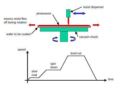
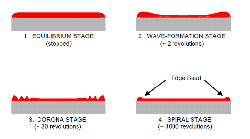
#* Wafer is held on a spinner chuck by vacuum and resist is coated to uniform thickness by spin coating. Resist thickness is set by primarily resist viscosity and secondarily spinner rotational speed. Most resist thicknesses are 1-2 mm for commercial Si processes. [[Image:HKU-HKBU_Photolithography_figure_1.png | frame | center | Fig 1 Photoresist Spin Coating]] [[Image:HKU-HKBU_Photolithography_figure_2.png | frame | center | Fig 2 Stages of Resist Coating]] | #* Wafer is held on a spinner chuck by vacuum and resist is coated to uniform thickness by spin coating. Resist thickness is set by primarily resist viscosity and secondarily spinner rotational speed. Most resist thicknesses are 1-2 mm for commercial Si processes. [[Image:HKU-HKBU_Photolithography_figure_1.png | frame | center | Fig 1 Photoresist Spin Coating]] [[Image:HKU-HKBU_Photolithography_figure_2.png | frame | center | Fig 2 Stages of Resist Coating]] | ||
| Line 158: | Line 158: | ||
# Post Processing Cleaning (Ashing) | # Post Processing Cleaning (Ashing) | ||
| - | Light Sources | + | '''Light Sources''' |
# Ultraviolet light from gas-discharge lamps | # Ultraviolet light from gas-discharge lamps | ||
| Line 165: | Line 165: | ||
# High-index immersion lithography (193nm) | # High-index immersion lithography (193nm) | ||
| - | Basics of Photolithography for Processing | + | '''Basics of Photolithography for Processing''' |
# Additive -> deposition | # Additive -> deposition | ||
| Line 172: | Line 172: | ||
[[Image:HKU-HKBU_Photolithography_figure_6.png | frame | center | Fig 6 Microfabrication Processes]] | [[Image:HKU-HKBU_Photolithography_figure_6.png | frame | center | Fig 6 Microfabrication Processes]] | ||
| - | Two primary techniques for patterning additive and subtractive processes | + | '''Two primary techniques for patterning additive and subtractive processes''' |
| + | |||
# Etch-back: | # Etch-back: | ||
#* photoresist is applied overtop of the layer to be patterned | #* photoresist is applied overtop of the layer to be patterned | ||
| Line 230: | Line 231: | ||
# Bruce W. Smith, "Resist Processing" in James R. Sheats and Bruce W. Smith eds., "Microlithography", Marcel Dekker (1998) | # Bruce W. Smith, "Resist Processing" in James R. Sheats and Bruce W. Smith eds., "Microlithography", Marcel Dekker (1998) | ||
# SEMI technical program, Semicon Europa (1996) | # SEMI technical program, Semicon Europa (1996) | ||
| - | |||
{{Team:HKU-HKBU/footer}} | {{Team:HKU-HKBU/footer}} | ||
Revision as of 05:39, 21 October 2009
Contents |
Protocols (in alphabetical order)
Bacteria Lysis
- Harvest the culture by centrifuge (13krpm*1.5min) followed by washing with 1ml PBS twice. Later steps should be done on the ice.
- Re-suspend the pellet with PBS (five times volume of the pellet) and protease inhibitor cocktail.
- Sonication for (5.5seconds+1second pulse)*10 minutes and protein solutions are obtained.
BCA Quantification Analysis
- Prepare a working solution of BCA reagent just prior to use by adding BCA Reagent A and BCA Reagent B with a ratio of 50:1. Mix the two solutions until a clear green solution forms. Prepare the BCA working reagent fresh daily. 100uL is required for each sample.
- For each protein determination, add 2~5uL protein sample and 100uL BCA mixture into each well. Usually each sample will be loaded into 3 wells to reduce errors.
- Put the 96-well plate in the warm room for about 30 minutes.
- Read the wells in a suitable plate reader (e.g. Molecular Devices) at the wavelength of 562 nm.
Competent Cell Preparation for Electro Transformation
- Materials
- Media: LB (Both liquid media and media containing agar. Add certain antibiotic if necessary.)
- Buffers and Solutions: 10% Glycerol.
- Special Equipments : EP tubes (1.5mL), micropipette tips, centrifugation bottles (polypropylene tubes, 50mL), graduated flask (250mL*2, 5mL*1), plates and test tubes.
- Steps
- Sterilization
- Including all materials in materials section.
- Caution (Remind): use some special marks to distinguish the sterilized materials from the unsterilized ones.
- Preparation after sterilization
- Chill the 10%Glycerin to 4°C.
- Decant LB containing agar into the plates.(If antibiotics are necessary, be sure that they are added when the media temperature is below 60°C.)
- Streak the prepared strains onto the agar plates. Then incubate it at 37°C for 10-16 hours.
- Pick up one single colony from the plate and pre-culture it overnight
- Take 0.5mL overnight culture to 50mL LB bottle.
- 37 centigrade degree shaking 100~120 min to O.D. (wavelength 600) 0.45~0.6
- On ice for 30min
- 4000rpm, 7min at 4 centigrade degree
- Add origin volume 10% glycerol, suspend softly.
- Repeat the step 7,8
- Add origin volume 1/10 10% glycerol, suspend softly.
- 4000rpm, 7 min at 4 centigrade degree
- Add origin volume 1/100 10% glycerol, suspend softly, store at -80°C.
- Sterilization
Electro Transformation
- Hold competent cells (from -80 centigrade degree refrigerator) on ice.
- Gently mix ligation product (1-5 µL) with cells.
- Transfer the cell/DNA mix into an electroporation cuvette. (Note: the gene pulser should already be set properly)
- Time constant = 4.5 - 5.0 ms
- Resistance = 200 W
- Capacitance = 25 mFD for 0.1 cm gap cuvettes, set the volts to 1.8 kV
- Pulse the cells once; the voltage display blinks, and the gene pulser beeps
- Quickly transfer 37°C SOC to cuvette, mix by gently pipetting up and down, and transfer SOC/cells back to culture tube.
- Bath in 37°C for 30~60 min.
- Separate cells on petri-dishes, and cultivate them in 37°C for 12-16 hours.
Ligation
England Biolabs T4 DNA ligases are used here.
- Choose reaction volume: 5-10 µL
- Mix proper proportion (usually 3~5:1) of DNA fragment and vector.
- Add 10 × ligase buffers.
- Add 0.5 µL ligase per 10 µL final volume.
- Bath in 16 centigrade degree water for 12 hour,
- Begin transformation.
Membrane Biotinylation
- Activate the membrane with methanol for 10-30seconds
- Balance the membrane in PBS for 5 minutes
- Place the membrane on a piece of filter paper.
- Drop the protein-biotin complex onto the membrane.
- Air-dry for 5 minutes.
- Soak in methanol for 1minutes.
- Place the membrane on a piece of filter paper.
- Air dry for 15 minutes.
Pre-culture
- One single colony is picked up from the agar plate and transferred to a tube.
- Add 3~5mL LB broth to the tube and the specific resistance.
- Culture overnight at 32 centigrade degree or 37°C.
Photolithography
The motors are fabricated by using a general surface manufacturing process for Si and SiO2. The motor bodies are made by reactive ion etching of thermal SiO2 layer on a Si substrate with a mask. Then the Si under the motors is anisotropically etched by wet etching, so that the motors are tethered to the Si base by two thin bridges designed to break upon sonication.
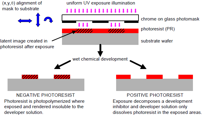
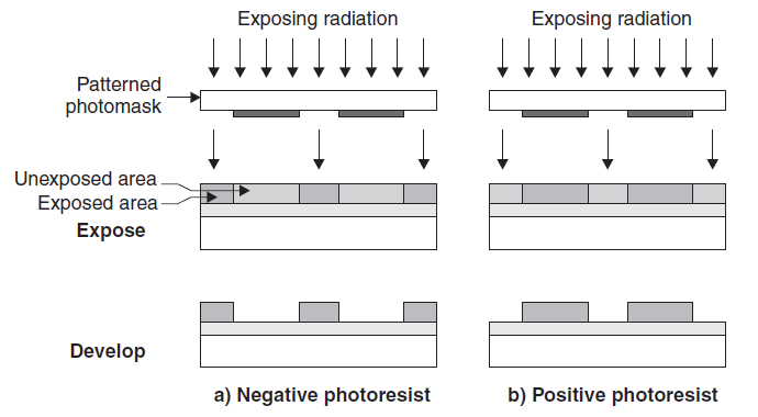
Photolithography is an optical means for transferring patterns onto a substrate. It is essentially the same process that is used in lithographic printing. Patterns are first transferred to an imagable photoresist layer. Photoresist is a liquid film that can be spread out onto a substrate, exposed with a desired pattern, and developed into a selectively placed layer for subsequent processing.
Overview of the photolithography process
- Surface Preparation
- Typical contaminants that must be removed prior to photoresist coating:
- dust from scribing or cleaving (minimized by laser scribing)
- atmospheric dust (minimized by good clean room practice)
- abrasive particles (from lapping or CMP)
- lint from wipers (minimized by using lint-free wipers)
- photoresist residue from previous photolithography (minimized by performing oxygen plasma ashing)
- bacteria (minimized by good DI water system)
- films from other sources:
- solvent residue
- H2O residue
- photoresist or developer residue
- oil
- silicone
- Wafer priming: Adhesion promoters are used to assist resist coating.
- Resist adhesion factors:
- moisture content on surface
- wetting characteristics of resist
- type of primer
- delay in exposure and prebake
- resist chemistry
- surface smoothness
- stress from coating process
- surface contamination
- Wafer primers
- Used for silicon:
- primers form bonds with surface and produce a polar (electrostatic) surface
- most are based upon siloxane linkages (Si-O-Si)
- 1,1,1,3,3,3-hexamethyldisilazane (HMDS), (CH3)3SiNHSi(CH3)3
- trichlorophenylsilane (TCPS), C6H5SiCl3
- bistrimethylsilylacetamide (BSA), (CH3)3SiNCH3COSi(CH3)3
- Used for gallium arsenide:
- GaAs already has a polar surface
- monazoline C
- trichlorobenzene
- xylene
- Used for silicon:
- Resist adhesion factors:
- Typical contaminants that must be removed prior to photoresist coating:
- Coating (Spin Casting)
- Wafer is held on a spinner chuck by vacuum and resist is coated to uniform thickness by spin coating. Resist thickness is set by primarily resist viscosity and secondarily spinner rotational speed. Most resist thicknesses are 1-2 mm for commercial Si processes.
- Pre-Bake (Soft Bake)
- Pre-bake is used to evaporate the coating solvent and to densify the resist after spin coating. Commercially, microwave heating or IR lamps are also used in production lines. Hot plating the resist is usually faster, more controllable, and does not trap solvent like convection oven baking.
- Alignment
- Exposure
- For simple contact, proximity, and projection systems, the mask is the same size and scale as the printed wafer pattern. I.e. the reproduction ratio is 1:1.
- Projection systems give the ability to change the reproduction ratio. Going to 10:1 reduction allows larger size patterns on the mask, which is more robust to mask defects.
- Mask size can get unwieldy for large wafers.
- Most wafers contain an array of the same pattern, so only one cell of the array is needed on the mask. This system is called Direct Step on Wafer (DSW). These machines are also called “Steppers”.
- Development
- Types:
- photographic emulsion on soda lime glass (cheapest)
- Fe2O3 on soda lime glass
- Cr on soda lime glass
- Cr on quartz glass (most expensive, needed for deep UV litho)
- Dimensions:
- 4” x 4” x 0.060” for 3-inch wafers
- 5” x 5” x 0.060” for 4-inch wafers
- Polarity:
- "light-field" = mostly clear, drawn feature = opaque
- "dark-field" = mostly opaque, drawn feature = clear
- Normally, this process requires at least two alignment mark sets on opposite sides of wafer or stepped region.
- Types:
- Post-Bake (Hard Bake)
- Post bake is used to stabilize and harden the developed photoresist prior to processing steps that the resist will mask. The main parameter of this process is the plastic flow or glass transition temperature. It can remove any remaining traces of the coating solvent or developer. Also, it eliminates the solvent burst effects in vacuum processing. Post-bake introduces some stress into the photoresist and some shrinkage of the photoresist may occur. Longer or hotter post-bake makes resist removal much more difficult.
- Processing Using the Photoresist as a Masking Film
- Photoresist will undergo plastic flow with sufficient time and/or temperature.
- Stripping
- This process is to remove the photoresist and any of its residues. Simple solvents are generally sufficient for non-postbaked photoresists. There are two kinds of photoresist, i.e. positive photoresist and negative photoresist. Besides, plasma etching with O2 (ashing) is also effective for removing organic polymer debris.
- Post Processing Cleaning (Ashing)
Light Sources
- Ultraviolet light from gas-discharge lamps
- "deep ultraviolet", produced by excimer lasers
- Immersion lithography with numerical apertures
- High-index immersion lithography (193nm)
Basics of Photolithography for Processing
- Additive -> deposition
- Subtractive -> etching
- Modifying -> doping, annealing, or curing
Two primary techniques for patterning additive and subtractive processes
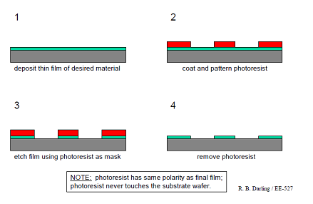
- Etch-back:
- photoresist is applied overtop of the layer to be patterned
- unwanted material is etched away
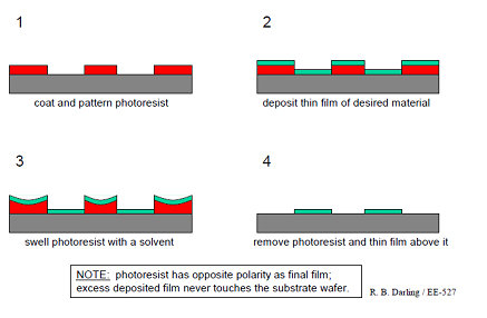
- Lift-off:
- patterned layer is deposited over top of the photoresist
- unwanted material is lifted off when resist is removed
Recombineering
- Overnight cultures: 5mL medium (containing antibiotic where applicable) from single colonies grown at 32°C for 18 h.
- Get 500uL from overnight cultures expanded into 50 ml of L medium in a 250 ml Erlenmeyer flask, and incubated at 32°C for 2h (until OD600 of ca. 0.4–0.6).
- Flasks were transferred to a shaking water bath at 42°C and incubated for 14–15 min, before cooling to 0°C as rapidly as possible in iced water.
- After 15–20 min, cells were harvested by centrifugation at 0°C (4000 g, 9 min).
- Cell pellets were carefully washed three times with sterilized ice-cold water (2 × 50 ml, then 1 × 1.5 ml) then re-suspended in 100–200 µl of ice-cold water.
- Competent cells (50 µl) were transformed with 50–200 ng of (gel purified) linear dsDNA targeting cassette using a BioRad electroporator (1.8 kV, 25 mF, 200 W).
- The LB medium (1 ml) was added to the transformed cell mixture, which was incubated at 32°C, for 2 h. Cells were collected by centrifugation, ca. 900 µl of supernatant media was discarded, and then the re-suspended cells were plated onto LB agar containing the appropriate antibiotic to select for resistant colonies. Reference to Watt et al [1].
SDS-PAGE and Western Blotting
- Buffer preparation
- Rususpension buffer: 1ml stock + 0.1ml protease inhibitor (10x)
- Loading buffer: 1ml stock + 0.2 ml DTT + Phenol Blue
- Sample treatment
- Centrifuge the culture into pellet (13k rpm 10min)
- Resuspend the pellet with 5xVolume(pellet) Resuspension buffer
- Add 5xVolume(pellet) loading buffer
- Boil the resuspend for 10 minutes at 100’C
- Centrifuge for 1 min at 13krpm
- SDS-PAGE
- 15% separation gel
- 5% stacking gel
- Load the sample and run under the constant voltage of 100V.
- Visualize your proteins using Coomassie Brilliant Blue, Silver stain, or any of the other protein stains or blot the gel for western blotting.
- Western blotting
- Transfer from gel to membrane
- Assemble "sandwich" Transblot.
- Prewet the sponges, filter papers (slightly bigger than gel) in 1x Blotting buffer.
- Transfer for 1 hr at 1 amp at 4°C on a stir plate. Bigger proteins might take longer to transfer. For the Mini-Transblot, it's 100 V for 1 hr with the cold pack and prechilled buffer. When finished, immerse membrane in Blocking buffer and block overnight.
- Hybridization with antibodies
- Incubate with primary antibody diluted in Blocking buffer for 60 min at room temp.
- Wash 3 x 10 min with 0.05% Tween 20 in PBS.
- Incubate with secondary antibody diluted in PBS for 45 min at room temp.
- Wash 3 x 10 min with 0.05% Tween 20 in PBS.
- Detect with SUPER SIGNAL WEST PICO Kit (1ml luminol solution + 1ml stable peroxide solution
- Result analysis
- The size of the tagged protein can be determined by the marker (protein ladder)
- The amount of the protein can be estimated by the brightness of the band, or accurately analyzed by the software.
- Trouble shooting
- Unspecific binding : 1st antibody-membrane and irrelevant protein to 1st antibody
- Film over-exposure or lack of exposure
Reference
- Watt RM, Wang J, Leong M, Kung HF, Cheah KS, Liu D, Danchin A, Huang JD. Visualizing the proteome of Escherichia coli: an efficient and versatile method for labeling chromosomal coding DNA sequences (CDSs) with fluorescent protein genes. Nucleic Acids Res. 2007, 35(6):e37.
- R. B. Darling / EE-527
- Bruce W. Smith, "Resist Processing" in James R. Sheats and Bruce W. Smith eds., "Microlithography", Marcel Dekker (1998)
- SEMI technical program, Semicon Europa (1996)
 "
"

